AND ALSO: The following procedure is done at your own risk.
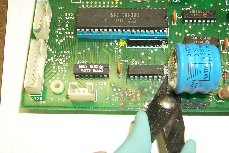
(A side note of amusement: The reddish stained area just below IC31 where the words "TO TAPE - GND - FROM TAPE - GNDA" are printed is actually the letters "OK" written by the original Korg employee who tested the KLM-367s when they were manufactured. The "OK" scribble appears at various places on these boards, but it is funny to see the board marked "OK" in the exact area that is damaged!)
Note the corrosion that has affected the large ground trace to the right of the solder blob where the black ground wire attaches. This trace is actually salvagable, but the smaller traces will have to be cut away and replaced by board-repair wire.
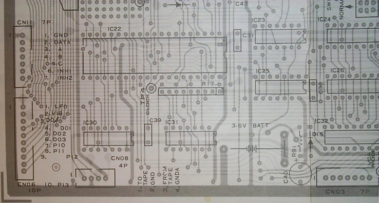
3-1: Using the following diagrams for reference, notice the color of the
"healthy" traces outsides the damaged area versus the blackened tracks
that are candidates for repair. The image on the right is from my
original Korg Polysix service manual, which I talked a Korg tech into
sending me in 1985. I will try to make an Adobe Acrobat version of the
entire manual available on this site at some point. This particular image
is part of the trace map for the KLM-367, which shows the routing of every
trace on the board. The darker-shaded traces are the "top" layer--that
is, the ones that can be seen in the image of the board on the left. The
lighter-shaded traces are on the bottom of the board, and should be
unaffected by the corrosion. Images of the bottom of the board will be
seen in later steps. The X-acto knife is used as a pointer, DO NOT
cut any traces at this time.

3-2: Now compare the image of the damaged area to the traces marked on
this modified image of the trace map. These are the traces chosen for
repair on this particular KLM-367.

All the traces marked in red indicate the traces that will be removed from the board. Note that all the red-marked tracks are on the "top" layer.
The areas marked in yellow indicate where the green soldermask is scraped away to expose the shiny, healthy copper so it can have a repair wire soldered to it. The large yellow area at the bottom already has solder on it from where the black ground wire attached.
The area marked in blue shows the blackened section of the large ground trace. This area was scraped to expose the copper in order to determine if the copper was still healthy enough to function. (In this board's case, it was considered healthy enough, and was thus left intact).
Look carefully at the marked trace map, and green dots can be seen where some of the parts were mounted as well as a number of the vias (little solder dots that have no parts or wires going to them). These green-marked pads are where a #70 drill bit in a dremel drill-press is used to bore out the holes after the solder is removed. On corrosion-damaged boards, the plated-through holes (there is a thin 'ring' of copper plating inside each hole, connecting the top and bottom layers) are the first thing to fail as they are not underneath a protective soldermask. Rather than risk intermittent operation from flaky hole plating, these holes are drilled out to allow the repair wires to easily be soldered in. Replacement parts do have to mount in some of the holes, however, and so care must be taken to save as much of the bottom-layer copper as possible.
The pads marked in orange show where parts are removed so the new battery can be installed. The resistor marked 'R91' is replaced by a diode, and the capacitor marked 'C40' is removed and the location left open. This is to allow the new Lithium battery (not an evil Ni-Cad) to work properly.
3-3: Take as much time as needed to determine which tracks to replace. This is the most difficult step in the procedure that doe not require actual soldering or cutting. A lot of care spent here will save a lot of time and headache later. Here are a few pointers to consider, but don't just take these tips at face value. Every board will have a different repair profile.
I tend to repair every top layer trace that touches IC31. Even if the tracks look healthy, the through-hole plating may not be conducting properly. Examine the solder and if it looks encrusted or crumbles when scraped at with a knife, consider that hole a suspect.
The first long vertical trace on the left, marked in red, I usually end up replacing. Check yours out, however. It may be OK.
The longest vertical trace marked in red that crosses over the lettering "3.6V" tends to need replacing. Check yours.
The thicker red trace with the bend to the right in it may be OK. The heavier tracks usually survive. If it looks suspect, scrape the blackening away to see if there is lots of shiny copper underneath. The short, very thick red trace that goes to the battery (-) pad is also probably OK. Check it out the same way. The thick trace that runs past the "B" in the "BATT" printed on the board also need to be checked out.
The four traces on the right, just above the right half of the blue area, usually do not need repair. The traces in this example did, but this is the case maybe 1 out of 20 times. Even so, check yours out. Notice that there are green dots marked for the holes of R17, a resistor array. I had to replace the resistor array on the board in this example, but again this part tends to hold up better than things like IC31. Check yours out. If the gunk can be scraped away to reveal shiny solder, it is likely in good shape.
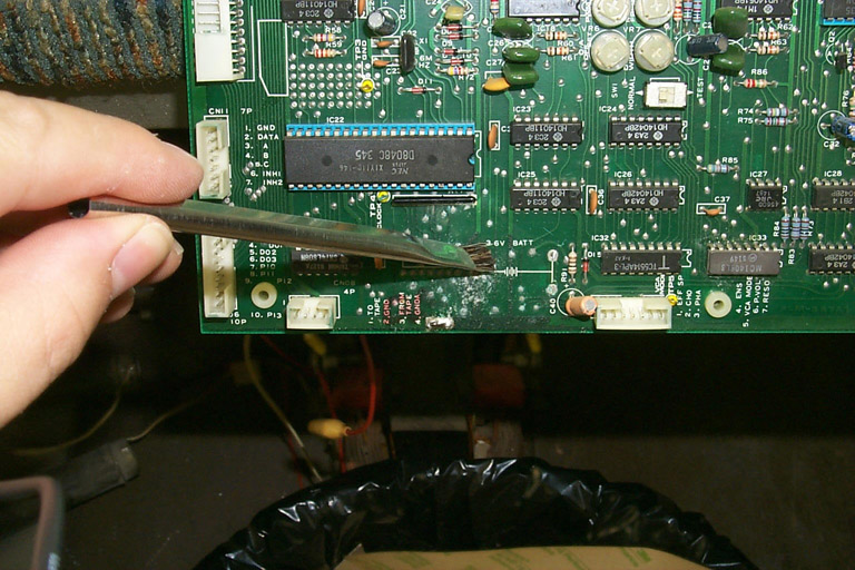
3-4: Using a clean brush, hold the board similar to the dry brushing image above and clean the damaged area with either alcohol, acetone (be careful with it) or if you can still get some, 1,1,1-trichloroethane, which was a popular board cleaning chemical.
3-5: Take a break. The trickiest part of the whole procedure is up next.